



10 Tips for Choosing the Best FPGA Chip?
Choosing the right Fpga Chip is a practical engineering decision, not a simple specification contest. Device selection affects clock stability, thermal behavior, board size, firmware effort, and future product upgrades. Ross Freeman, Xilinx co-founder and FPGA pioneer, famously described the FPGA as “a blank canvas for digital designers.” That canvas still needs the right dimensions, materials, and tools.
This guide presents 10 Tips for Choosing the Best FPGA Chip, based on real design priorities. It examines logic capacity, lookup tables, flip-flops, memory blocks, DSP resources, transceivers, package options, power consumption, and development support. A laboratory prototype may tolerate unused pins or excessive resources. A production board cannot. Every extra watt can raise enclosure temperature. Every unsupported interface can delay testing by weeks. Small details matter.
The process should begin with the workload, not the most impressive product brochure. Define required data rates, operating temperatures, latency limits, and expected product life. Then compare devices using verified datasheets, reference designs, evaluation boards, and independent measurements. Vendor claims are useful, but they are not the whole truth. Some choices will remain uncertain until timing closure or thermal testing. That is normal. I have seen designs that looked perfect on paper fail because one clock domain was underestimated. These tips aim to reduce that risk while leaving room for honest engineering judgment.
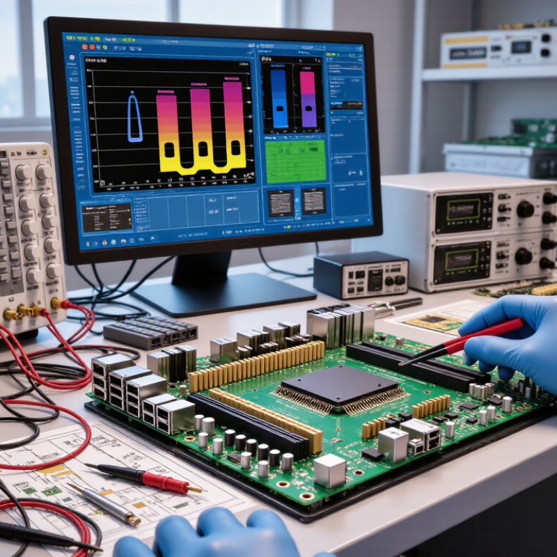
Specify the Workload: Translate Throughput, Latency, and 100–1,000 MHz Clocks
Choosing an FPGA starts with the workload, not the device name. Define throughput, latency, and clock targets in measurable terms. A 256-bit datapath at 250 MHz carries 64 Gb/s before protocol overhead. At 1,000 MHz, a 64-bit path reaches the same raw rate. The arithmetic is simple. Real designs are not.
Measure latency in clock cycles and nanoseconds. Twenty cycles at 500 MHz equal 40 nanoseconds. However, buffering, memory access, arbitration, and clock-domain crossings add delay. I often estimate too optimistically here.
A practical margin of 20–30% can prevent painful redesigns, although the correct margin depends on traffic patterns. Test burst and idle conditions separately. Average throughput can hide short stalls.
Market pressure makes this discipline more important. The World Semiconductor Trade Statistics Spring 2024 forecast projected global semiconductor sales of 611 billion dollars in 2024, a 16% annual increase. International Data Corporation’s 2024 edge-spending guidance projected worldwide edge investment above 230 billion dollars, with continued growth through 2027. These trends increase demand for responsive processing near sensors and machines.
Translate that demand into samples per second, bytes per transfer, and worst-case response time. Then check whether the FPGA offers enough DSP resources, memory bandwidth, and transceiver capacity at 100–1,000 MHz. Do not trust the headline clock. Sustained timing closure may require a slower, wider pipeline. That trade-off is easy to miss.
Size the Fabric: Compare 10K–2M+ Logic Cells, DSPs, and 10–100+ Mb BRAM
Sizing the FPGA Fabric: Logic Cells, DSPs, and BRAM
Start with the workload, not the largest available device. A small control design may fit inside 10K logic cells, while a vision pipeline can demand 2M+ cells. Count registers, lookup tables, interfaces, and control logic after synthesis. Leave room for timing fixes and late feature changes. Headroom matters.
DSP capacity deserves equal attention. Multipliers, filters, and matrix operations can consume hundreds of DSP blocks quickly. Estimate operations per clock, then check whether the fabric can meet your target frequency. A design with enough logic cells may still fail because its DSP columns are exhausted. That mistake is expensive.
Memory planning often exposes hidden limits. Compare on-chip BRAM from roughly 10 Mb to more than 100 Mb, based on buffering, line storage, firmware, and data width. Calculate simultaneous reads and writes, not only total capacity. A 64-bit pipeline can waste memory when the available block width is narrower. External memory may solve capacity, but it adds latency and board complexity.
Review post-synthesis and post-route reports before committing. Logic-cell estimates can shift after optimization, especially with wide buses and deep pipelines. I have seen early spreadsheets look comfortable, then collapse under routing congestion. Do not trust a single estimate. Measure twice. Allow practical margin for temperature, timing closure, and future revisions.
FPGA Capacity Comparison: Logic Cells, DSP Blocks, and BRAM
Representative FPGA capacity tiers range from approximately 10,000 to more than 2 million logic cells. As device size increases, available DSP blocks and embedded block RAM typically scale as well, supporting larger signal-processing, memory-intensive, and parallel-computing designs.
Match Interfaces: Evaluate 1–112 Gbps Transceivers and DDR4/DDR5 Support
Tip 1 Match the FPGA’s interfaces to your real data path, not just the headline speed. Transceivers from 1 to 112 Gbps serve very different design goals. A short control link may need low power, while a backplane requires stronger signal integrity and equalization. Check lane count, encoding overhead, connector loss, and usable throughput. A 112 Gbps link does not deliver 112 Gbps of payload automatically.
Tip 2 Treat DDR4 and DDR5 support as a system decision. Compare memory speed, channel width, capacity, training features, and controller availability. DDR5 can provide higher bandwidth, but it may increase layout sensitivity and power demands. Keep traces short and matched. During a recent evaluation, our first bandwidth estimate looked excellent, but arbitration and refresh reduced actual performance. That mistake changed our testing method.
Tip 3 Validate interfaces with hardware evidence before committing to production. Review reference layouts, timing margins, thermal data, and transceiver compliance reports. Measure eye openings under realistic traffic, not only idle patterns. Also test startup behavior and clock stability. Engineers sometimes choose the fastest interface and discover that the board cannot route it cleanly. A slower link can be more reliable. Document those trade-offs clearly, including assumptions that may later prove wrong.
Optimize Power and Cost: Weigh 7–28 nm Nodes, TDP, Package, and Volume
Choosing the best FPGA chip starts with power and cost, not logic-cell count alone. A 7 nm device can reduce dynamic power, but its advanced process may increase mask costs, leakage sensitivity, and minimum order requirements. A 16 nm or 28 nm option can be cheaper for moderate workloads. Smaller is not automatically better.
The International Energy Agency reported that data centers used about 415 TWh globally in 2024, making energy efficiency a serious design constraint. Measure real TDP under your workload, not only the vendor’s typical figure. Add memory, transceivers, regulators, and cooling losses. A 25 W FPGA may require a larger heat spreader than expected. Package choice matters too: larger packages improve I/O and thermal transfer, but raise board area and assembly costs. I have seen prototypes fail budget reviews because package pricing was ignored.
Volume changes the decision. Industry forecasts from the World Semiconductor Trade Statistics organization projected global semiconductor sales near 697 billion dollars in 2025. High-volume products can justify newer nodes and custom thermal designs. Low-volume equipment may benefit from mature 28 nm supply and simpler qualification. Check lifecycle data, package availability, and lead-time history. My own early estimates have been too optimistic before. Real thermal tests and three-year supply quotes are worth the extra week.
10 Tips for Choosing the Best FPGA Chip? - Optimize Power and Cost: Weigh 7–28 nm Nodes, TDP, Package, and Volume
Comparative planning guide for selecting an FPGA by process node, thermal design power, package, production volume, and system requirements.
| Tip | Selection Dimension | What to Check | 7 nm Class | 12–16 nm Class | 22–28 nm Class | Cost and Power Implication | Recommended Decision |
|---|---|---|---|---|---|---|---|
| 1 | Define the workload first | Estimate logic cells, memory bits, DSP blocks, high-speed transceivers, I/O count, and required operating frequency. | Best for very high logic density, advanced networking, intensive signal processing, and demanding acceleration. | Balanced option for high-performance embedded processing, communications, industrial vision, and edge systems. | Suitable for control logic, moderate signal processing, industrial interfaces, and cost-sensitive designs. | Oversizing the device increases silicon, package, power, and development costs. | Select the smallest device that meets resource needs with at least 20% practical capacity margin. |
| 2 | Compare process nodes | Review density, voltage domains, static power, performance, availability, qualification status, and design-tool support. | Highest density and performance potential | Strong balance of density, maturity, and cost | Mature, economical, and often easier to source | Smaller nodes can reduce energy per operation but may increase non-recurring engineering and package costs. | Choose a 7 nm class only when density, bandwidth, or performance justifies the premium. |
| 3 | Set a realistic TDP target | Evaluate static power, dynamic power, clock frequency, utilization, transceiver activity, memory traffic, and ambient temperature. | Representative planning range: approximately 15–75 W for high-end devices, depending heavily on configuration. | Representative planning range: approximately 8–55 W across mid-range and high-end devices. | Representative planning range: approximately 2–30 W for many low- and mid-range applications. | TDP is application-dependent; a process node alone does not determine total board power. | Calculate power from an actual design estimate rather than relying only on a device-family maximum. |
| 4 | Check thermal headroom | Confirm junction-temperature limits, heat-spreader requirements, airflow, heatsink size, and enclosure restrictions. | Often requires controlled airflow, a heat spreader, or a carefully designed thermal path at high utilization. | May support passive or moderate forced-air cooling in many embedded designs, subject to workload. | Frequently easier to cool passively, especially when clock rates and transceiver use are moderate. | Thermal hardware can materially affect the total system cost and mechanical design. | Reserve thermal margin for hot ambient conditions, aging, and workload bursts. |
| 5 | Match the package to the PCB | Compare ball count, pitch, package footprint, layer count, escape routing, power delivery, and assembly capability. | Advanced devices commonly use large, high-density packages with demanding breakout and power-integrity requirements. | Offers a broad range of package sizes and is often easier to integrate into performance-oriented boards. | More options may be available for compact, low-layer-count, and cost-sensitive boards. | A smaller die does not necessarily mean a smaller or cheaper package. | Approve the package only after PCB stack-up, escape routing, and assembly feasibility are verified. |
| 6 | Budget high-speed interfaces | Verify lane count, protocol support, line rate, reference-clock requirements, equalization, and signal-integrity margin. | Typically preferred for the highest aggregate bandwidth and advanced serial-interface requirements. | Often sufficient for multi-gigabit communications, video, storage, and industrial networking designs. | Appropriate when interface speed and lane count are moderate and protocol requirements are stable. | High-speed transceivers can increase power, PCB complexity, validation effort, and test cost. | Count active lanes and bandwidth before paying for a larger device or newer node. |
| 7 | Evaluate external memory needs | Check memory bandwidth, controller availability, supported memory types, signal integrity, and refresh or calibration requirements. | Well suited to bandwidth-intensive designs when the device and board can support advanced memory interfaces. | Good fit for substantial DDR-based buffering, image processing, and embedded compute workloads. | Can be economical when on-chip memory and moderate external memory bandwidth are sufficient. | Memory devices, routing, termination, and power delivery can outweigh the FPGA price difference. | Size memory for peak traffic, not only average throughput. |
| 8 | Consider production volume | Estimate annual units, product lifetime, approved-source requirements, inventory policy, and expected price sensitivity. | Usually easier to justify in high-value products where performance or density creates measurable system value. | Often attractive for medium-to-high volume products requiring a balance of features and cost. | Frequently competitive for high-volume, long-life, and cost-sensitive equipment. | Unit price should include PCB changes, cooling, software migration, validation, and inventory carrying cost. | Use total cost of ownership rather than comparing semiconductor prices alone. |
| 9 | Verify lifecycle and supply risk | Review published longevity, wafer and package availability, lead-time history, qualification requirements, and second-source options. | Can provide excellent performance but may involve more complex supply planning and advanced-package constraints. | Often offers a practical compromise between modern capability and manufacturing maturity. | Mature nodes may provide useful lifecycle advantages, but product availability must still be checked individually. | Unexpected obsolescence or long lead times can exceed the initial device-cost savings. | Obtain written lifecycle and supply information before design freeze. |
| 10 | Validate tools and migration effort | Assess synthesis quality, timing closure, IP availability, licensing, debugging tools, security features, and team experience. | May deliver the best performance but can require advanced power planning, timing closure, and implementation expertise. | Commonly provides a manageable balance of tool maturity, performance, and design complexity. | Can reduce migration risk for established designs, although older interfaces and tools must be verified. | Engineering hours, IP licenses, verification, and certification can dominate the project budget. | Prototype the most critical functions before committing to the final node and package. |
Validate the Platform: Check Toolchains, IP, 5–15-Year Availability, and Safety
When I evaluate an FPGA platform, I start with the development environment, not the silicon alone. Can engineers compile, simulate, debug, and update designs without fragile workarounds? A fast demonstration is not proof. Ask for versioned tool support, active documentation, and realistic build times. Check whether the required IP is mature, licensed clearly, and supported across the product’s expected life. Hidden integration effort can consume months.
Review the architecture’s five-to-fifteen-year availability plan. Confirm production history, supply commitments, and acceptable replacement paths. Request written evidence, not optimistic forecasts. I once trusted a long availability statement without checking package changes. That mistake forced a late redesign. The lesson stayed with me. Platform validation must include procurement and engineering teams.
Safety needs practical evidence. Look for diagnostic features, fault handling, traceability, and development processes aligned with applicable safety requirements. Examine how failures are detected, isolated, and recorded during testing. A polished safety claim means little without reviewable records and qualified personnel. Do not treat certification as a substitute for system analysis. A missing assumption can become a field problem. Leave room for independent assessment, because even experienced teams overlook uncomfortable details. When the toolchain, IP, supply plan, and safety evidence agree, the platform becomes easier to trust under real operating pressure.


